These signal plots were made by Gerrit Heitsch (gerrit (at) laosinh.s.bawue.de),
2011-11. Thanks Gerrit!
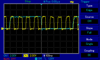
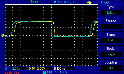
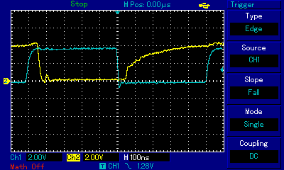
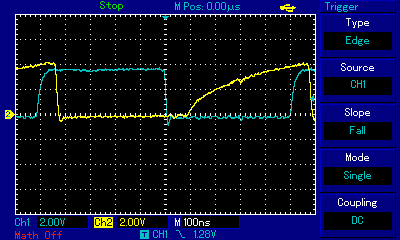
The first image is from a machine with 250466 board, 6510 CPU, 6569R5 VIC, and 82S100 PLA.
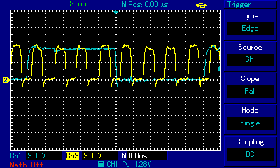
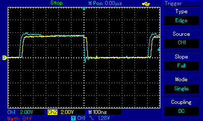
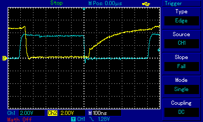
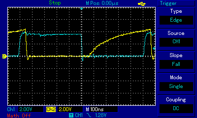
The second image is from a machine with 250469 board, 8500 CPU, 8565R2 VIC, and custom CMOS chip as "PLA".
Channel 1 (cyan) is the Phi0 clock in all these plots.
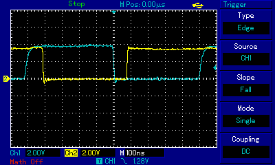
Let's first look at the Phi0 the VIC generates from the dot clock:
If everything in the circuits would happen instantaneously, the falling edge
of the dot clock would coincide with the falling edge of Phi0. From these
plots, you see that the delay on the old chip is almost twice what it is on
the new chip (half a pixel and a quarter pixel, respectively). The various
clock signals internal to the VIC should agree with Phi0 quite well (the
pin driver is rather fast and outputs the internal clock directly).
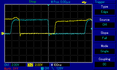
The CPU accesses the bus when AEC is high. A write to the VIC registers
will (in normal configuration, CPU port P2..P0 = 111 and the cartridge
detect pins high as well) be decoded to the VIC #CS pin by the core logic
(82S100 followed by a 74LS139, resp. a custom CMOS chip) from A15..A12 and
R/#W:
|
AEC |
 |
 |
|
R/#W |
 |
 |
|
A12 |
 |
 |
|
I/O #CS |
 |
|
|
VIC #CS |
 |
 |
The AEC signal already is behind a bit on the old chip, especially if you
look at the rise/fall time. This causes R/#W and the address lines (both
generated by the CPU) to be later as well, but no further delay here.
The PLA is slower than the CMOS chip, and the 74LS139 adds more delay;
in the end, the VIC #CS signal is about 35ns earlier on the new system.
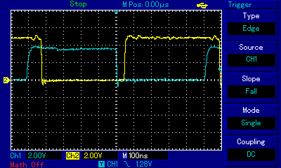
As a result, when writing to a VIC register the internal VIC logic starts
the write before the value is on the internal data bus, that data bus is
precharged instead; when writing to a colour register that is currently
being displayed, that shows colour 1111 (i.e. light grey) for a fraction
of a pixel before showing the written value (even if that is the same as
was in the register originally).